Semiconductor? IC?
"The semiconductor is a vital component. In terms of familiar items, it is mainly used in the so-called 3Cs-computers (information technology, including scanners, and so on), consumer electronics (such as full color video displays, micro-computer home appliances), and communications (mobile phones, wireless phones, etc.)," explains Hwang Chin-yeong of the Market Intelligence Center at the Institute for Information Industry. However, the range of applications of the silicon wafer is expanding constantly, with rapid growth in the fields of machine automation, national defense, and transportation.
The main user of semiconductors today is the information industry, which absorbs nearly one-third of the world's semiconductors. In Taiwan, where the information industry is one of the economy's strong suits, that industry accounts for 80% of Taiwan's total semiconductor use.
Categorized by product type, semiconductors can be divided into IC, discrete component, and optoelectronic types. Last year ICs accounted for 87% of the world's US$140 billion semiconductor market. However, one should not overlook the potential of optoelectronic semiconductors, which are a new product.
In Taiwan, optoelectronic semiconductors-used mainly in high resolution liquid crystal displays-are still in the preliminary stage. Thus, if you mention "Taiwan's thriving semiconductor industry," a nit-picking person may correct your terminology: "It would be more accurate to say 'Taiwan's IC industry'!"
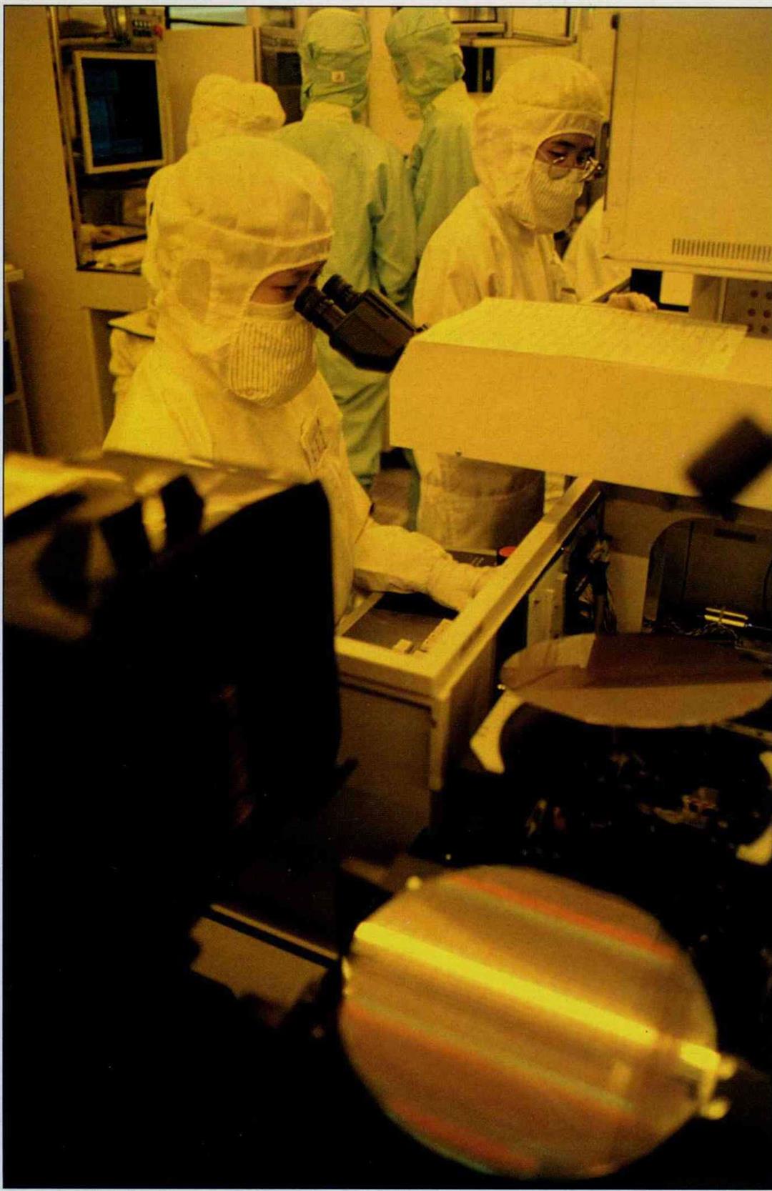
Whether optoelectronic or IC, both are semiconductors, and their manufacturing principles are more alike than different. These "semiconductor genies" appear on tiny "dies." These chips are mass-produced on "wafers" of 4, 5, 6, or 8 inches in diameter. A tour of a micron manufacturing plant for eight-inch wafers is truly an "amazing journey."
Just entering the plant is a major project. Check out some of the spine-tingling requirements from a long, long list: Makeup is prohibited (as makeup particles can seriously impair the conductivity of the circuits). Please use the restroom before beginning the tour (otherwise, like the employees, you'll have to "wait until the shift is over" to take care of your needs).
Before entering the "clean room," one must wash one's hands three times with water that is more pure than distilled water. One must then take dust-free coveralls out of a vacuum bag, wear a dust-free cap that covers all but the eyes, and wear dust-resistant footwear that go above the calf, thus thoroughly wrapping yourself up. Hot air from one's breath, trapped by a two layer face mask that pinches the bridge of the nose, immediately causes eyeglasses to fog up. Even note paper must be special-unusual long-fiber paper-in order to insure that no paper fibers drop off.
Small room, giant attraction
Upon entering the clean room, you see large machines in a row: The "ion implant machine" lays a membrane on the chip. Then, in a process called photolithography, the circuit design is projected onto the surface using glass "photomasks." Then the chip goes into the "etch" process, where areas of excess metal (i.e. metal which is outside the design projected on to the chip) are chemically eroded away. What is left is are rows of oblong dies.
Around and around it goes-design, photolithography, etching-in a repeated cycle. Every procedure must be repeated more than 20 times, with a different circuit design overlaid on the chip each time. Only after more than 50 days of the most precise etching can a single glittering eight-inch wafer of several hundred memory chips be successfully completed.
After all that comes a series of procedures for testing, cutting, and packaging. In this final stage the dies are wrapped in a black hard shell, out of which stick a number of "feet" for linking up with other circuits. Together these make up the ICs that we can see on the motherboards when we open up our computers.
Although virtually the entire process takes place in tightly sealed machines and operations are run by computer, so the chips are not exposed to air, there can still be no relaxation in the cleanliness measures of the clean room.
Looking down below one's feet, beneath the raised, nearly one-story high floor, there is a dense network of air vents. Based on the principle of air circulation, these absorb any particles out of the air which is re-circulated through the clean room. In this room, guests dare not move capriciously (for fear of stirring up particles), squeeze close together (for fear of causing the particle density in a certain space to exceed the limits), nor cough (for fear of having the same thing happen to them as happened to the character in the film Disclosure who was fired by his high-tech company for a 'drop in the cleanliness of the air').
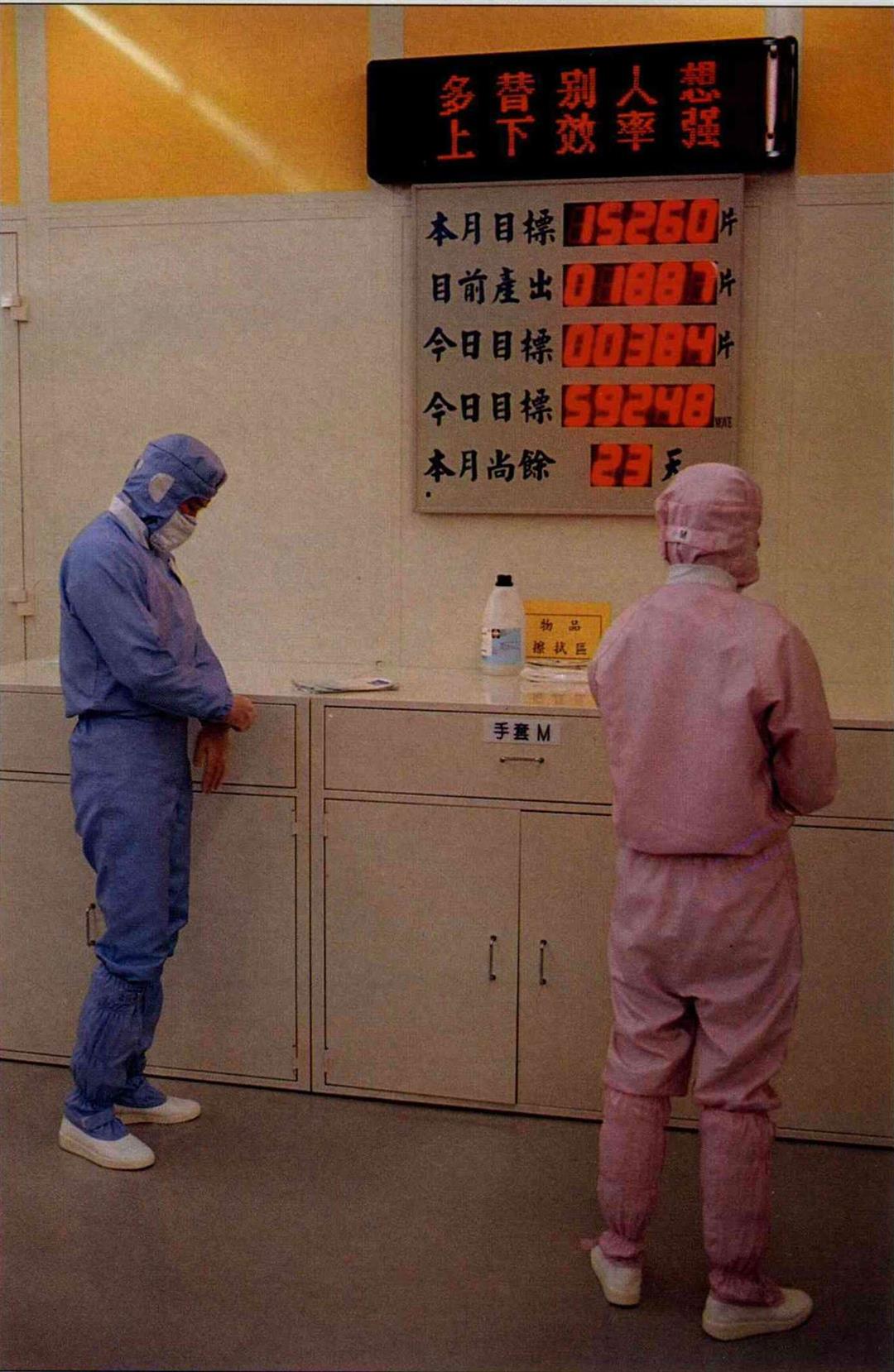
One noteworthy, and rather unexpected thing, is that this clean-room air which is "1000 times more pure than outside air"-in which even filtrable viruses find it hard to survive-does not make one feel refreshed and energetic. On the contrary, after a short period you feel stifled and dizzy. You really have to admire those women production line workers who spend 12 hours a day in there.
Stick close, but not too close
The item being manufactured in this first submicron manufacturing plant in Taiwan is the DRAM (dynamic random access memory), the most commonly used component in IC manufactured goods. Its life depends on immaculate production. But why?
Hu Chang-shung, supervisor in the manufacturing department at Vanguard International Semiconductor, who is leading the guests around, explains: The term submicron refers to anything below 1.0 micron (one-millionth of a meter). Given that a human hair is about seven microns in diameter, something in the submicron range is only a fraction of that size. This invisible-perhaps unimaginable-width is the smallest achievable distance between lines of metal on a chip (the "process dimension"). As Hu says, describing the difficulty of the submicron manufacturing process, "they have to be close, but not too close."
What he means by the phrase "stick close" is that the process dimension must be at the absolute minimum. Thus it is possible to pile up more than 20 layers on a glossy chip of only 2mm in length by 1mm in width by 0.5mm in height. Each layer, in turn, has hundreds of densely packed circuits etched into it.
The 16 Mb DRAM produced in this way is of startling capacity. It has 16 million bits of memory. If you figure that each Chinese ideographic character requires two bytes, then it can record millions of characters, or the equivalent of the Chinese language version of the Encyclopedia Brittanica. The ever-smaller and more densely packed memory is the secret recipe for more compact computers with increasingly large memory capacity.
On the other hand, the process dimension being so minuscule as it is, there is the risk of contact. Once there is contact, there is the possibility of a short-circuit. Besides defects in the manufacturing process itself, another cause of sticking is particles from outside. Sticking is fatal to a US$7 16 Mb DRAM chip. One 8-inch silicon wafer can hold hundreds of chips. The "yield rate" (the percentage of good chips on a wafer) is critical to profits and reputation, and is often one of the most carefully guarded secrets of a factory.
Extremely strict cleanliness management and quality control are what make sub- micron manufacturing so expensive. In contrast, things like sound chips-having fewer circuits-require less rigorous methods, with process dimensions as large as a micron or so.
Nevertheless, there's no limit to the challenges that those in the field have the ambition to tackle. As yet, 0.18 "deep submicron" technology is immature, and cannot yet go into mass production. But there are already people forecasting that a factory capable of producing a one gigabit chip at a process dimension of 0.1 micron will be up and running by the year 2000. At that time, we really will have the world on a string, and people's dreams can move further forward.