
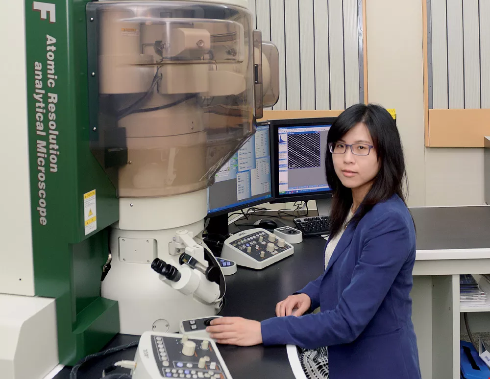
“There are so few female scientists that we’re easy to remember,” says 30-year-old Chou Yi-chia, an assistant professor in the electrophysics department of National Chiao Tung University. She adds that her gender has never made a difference in how her colleagues treat her, but it has helped her stand out from the crowd in a male-dominated field.
Chou became the youngest scholar at NCTU ever to have a paper published in the internationally renowned Science magazine when her “Atomic-Scale Variability and Control of III-V Nanowire Growth Kinetics” appeared in the journal in early 2014.
What exactly are “III-V nanowires”? How did Chou arrive at this inspiring breakthrough?
Chou Yi-chia turns the stereotype of the mannish, too-nerdy-for-makeup female scientist on its head. With her shoulder-length hair, short skirt, and heels, the graceful Chou is entirely feminine.
She has enjoyed an outstanding academic career, from the gifted program in mathematics and the sciences at Chia-yi Girls’ Senior High School to the undergraduate program in the Department of Materials Science and Engineering at National Tsing Hua University and through her graduate studies at the University of California, Los Angeles.
She was hired by IBM’s Thomas J. Watson Research Center after completing her PhD. As one of the center’s postdoctoral researchers, she immersed herself in the study of nanowire growth kinetics. She has continued that research since returning to Taiwan to take up a teaching position at National Chiao Tung University.
Chou Yi-chia’s fascination with the nanoscale world may well change the future.
The subject matter of Chou’s “Atomic-Scale Variability and Control of III-V Nanowire Growth Kinetics” may seem a bit abstruse, but nanoscale components are already a fact of life in everyday items such as computers and cellphones.
Chou explains that pushing the state of the art into nanoscale technology allows components to be packed more closely together on semiconductor wafers, which increases their efficiency and may well lead to next-generation technologies in the semiconductor, computing, and biomedical device industries.
Chou works on “III-V group” materials, which are compounds formed from the Group III and Group V elements on the periodic table of elements (there are eight groups in total).
She says that at the same width, wires made from Group III-V materials have higher electron mobility and waste less power than those made from Group IV materials. Scientists have been researching these materials in recent years in the hope that they will eventually replace silicon in semiconductors. The gallium phosphate (GaP) Chou studies is a case in point.
Currently, most nanowires are manufactured via lithographic processes that involve etching pathways into a substrate. With self-assembly, atoms instead form themselves into nanowires by deposition.
“Lithography is already at its limit. Self-assembly offers a way to push forward, allowing us to achieve higher resolutions and even smaller components,” explains Chou.
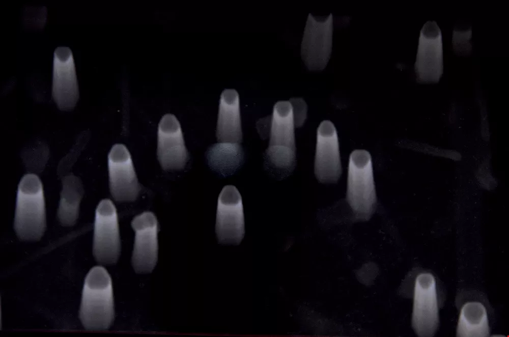
Under a microscope, growing GaP nanowires look like miniature art works. IBM’s Thomas J. Watson Research Center presented Chou with the photos to commemorate her efforts there.
Chou began working with the GaP nanowire self-assembly team at IBM’s Thomas J. Watson Research Center in August 2011. She has spent the last two years looking for atomic-scale self-assembly mechanisms for nanowires.
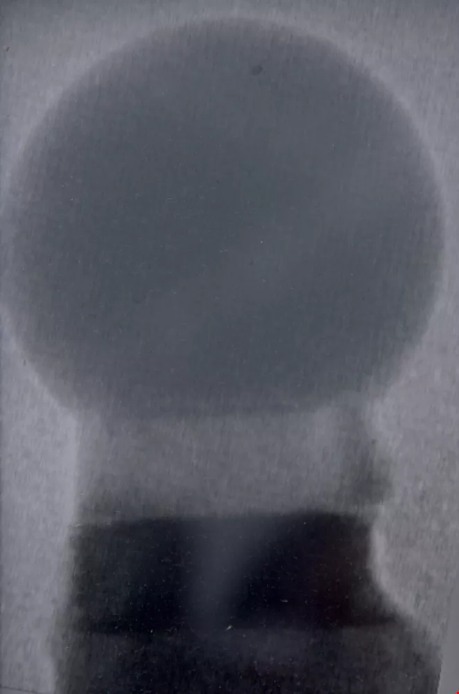
She conducts her experiments in an ultra-high vacuum electron microscope. Her method involves first placing a catalyst atop a three-micron-long silicon substrate, then using the vapor–liquid–solid growth process, which involves introducing trimethylgallium and phosphine. The nanowires then self-assemble atop the catalyst.
Chou says that with any given experiment, it’s impossible to know whether nanowires will grow or how long they’ll grow for. In some cases, they continue growing for as long as eight or nine hours. Since experimenters have to remain at the microscope the entire time to observe and take notes, they often miss lunch and dinner.
Her research has revealed that the rate of growth of the atomic layers of bicrystal GaP nanowires is extremely variable even in fixed and stable conditions.
Why?
In her search for answers, Chou filmed the entire growth process at 30 frames per second, then studied stills from these films to look for changes. She eventually discovered that transformations in the crystals’ structures accelerate the wires’ growth rate.
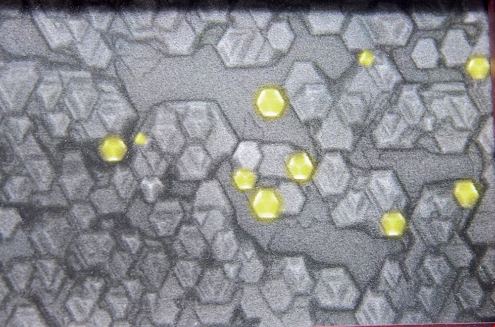
Under a microscope, growing GaP nanowires look like miniature art works. IBM’s Thomas J. Watson Research Center presented Chou with the photos to commemorate her efforts there.
Chou says that it’s going to be some time before the results of her research find applications in the nanoscale elements of semiconductors, computers, and biomedical devices.
Moving forward, she plans to continue her experiments while also training students. She says that her transnational cooperation with IBM is still moving ahead as well.
There are no gender distinctions in science. But someone putting Chou under the microscope looking for differences between female scientists and their male counterparts might note her powerful, feminine attachment to home and family.
“The six years I spent studying and working abroad cost me a lot of time away from my family.” Chou explains that her younger sister was still in elementary school when she went abroad, but was already a university student when she came back. Her parents had become much grayer as well.
In Chou’s mental calculus, family is just as important as professional success.
Under a microscope, growing GaP nanowires look like miniature art works. IBM’s Thomas J. Watson Research Center presented Chou with the photos to commemorate her efforts there.


